PCBend: Light Up Your 3D Shapes With Foldable Circuit Boards
Marco Freire*1, Manas Bhargava*2, Camille Schreck1, Pierre-Alexandre Hugron1, Bernd Bickel2, Sylvain Lefebvre1
*Joint first authors
1Université de Lorraine, CNRS, Inria, LORIA, France
2ISTA (Institute of Science and Technology Austria), Austria
SIGGRAPH 2023, DOI: 10.1145/3592411
Abstract
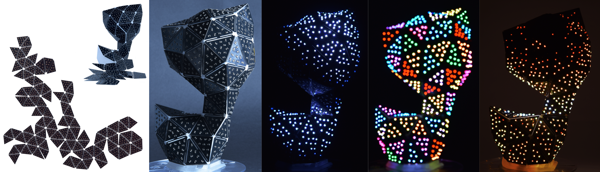
We propose a computational design approach for covering a surface with individually addressable RGB LEDs, effectively forming a low-resolution surface screen. To achieve a low-cost and scalable approach, we propose creating designs from flat PCB panels bent in-place along the surface of a 3D printed core. Working with standard rigid PCBs enables the use of established PCB manufacturing services, allowing the fabrication of designs with several hundred LEDs.
Our approach optimizes the PCB geometry for folding, and then jointly optimizes the LED packing, circuit and routing, solving a challenging layout problem under strict manufacturing requirements. Unlike paper, PCBs cannot bend beyond a certain point without breaking. Therefore, we introduce parametric cut patterns acting as hinges, designed to allow bending while remaining compact. To tackle the joint optimization of placement, circuit and routing, we propose a specialized algorithm that splits the global problem into one sub-problem per triangle, which is then individually solved.
Our technique generates PCB blueprints in a completely automated way. After being fabricated by a PCB manufacturing service, the boards are bent and glued by the user onto the 3D printed support. We demonstrate our technique on a range of physical models and virtual examples, creating intricate surface light patterns from hundreds of LEDs.
Citation
@article{freire:hal-04129354,
  TITLE = {PCBend: Light Up Your 3D Shapes With Foldable Circuit Boards},
  AUTHOR = {Freire, Marco and Bhargava, Manas and Schreck, Camille and Hugron, Pierre-Alexandre and Bickel, Bernd and Lefebvre, Sylvain},
  URL = {https://inria.hal.science/hal-04129354},
  JOURNAL = {ACM Transactions on Graphics},
  PUBLISHER = {Association for Computing Machinery},
  YEAR = {2023},
  DOI = {10.1145/3592411},
  KEYWORDS = {PCB design ; PCB bending ; automated placement and routing ; 3D electronics},
  PDF = {https://inria.hal.science/hal-04129354/file/main.pdf},
  HAL_ID = {hal-04129354},
  HAL_VERSION = {v1},
}
Acknowledgements
We thank the reviewers for the valuable feedback. We also thank the Miba Machine Shop at ISTA, PCBWay, and PragoBoard for helping us with fabrication and assembly. This project was supported by the European Research Council (ERC) under the European Union’s Horizon 2020 research and innovation program (Grant Agreement No. 715767 -– MATERIALIZABLE).

![]()
Resources
- Article
- Video
- Code and data: coming soon!